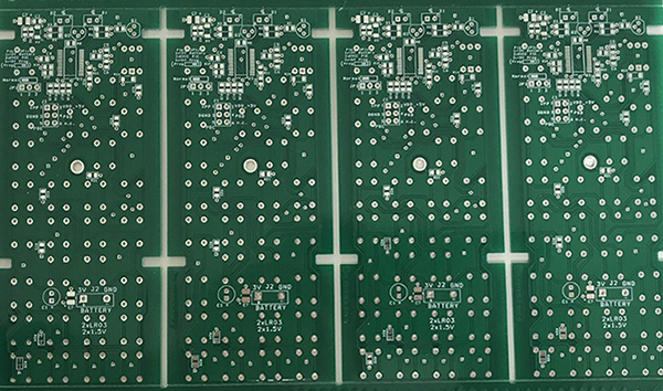
The chemical tin plating process is a non-electroplating process that deposits tin on the surface of copper. Its working principle is to use the higher activity of tin than copper in acid solution, so that a displacement reaction occurs between the copper foil of the pad and the tin ions in the tin plating tank, and the tin is oxidized to form a uniform tin layer.
Displacement reaction equation of the tin plating process:
Cu(s) + Sn2+(aq) → Cu2+(aq) + Sn(s)
In the equation, Cu represents copper, Sn represents tin, s represents solid, aq represents aqueous solution. In the reaction, the ion of copper is replaced by the ion of tin, forming a solid tin layer.
Comparison with the spray tin (hot air leveling) process:
The spray tin process sprays molten tin powder onto the surface of the substrate through a high-pressure nozzle. The thickness and uniformity of the tin layer are not as good as the immersion tin process, so it may not be suitable for some applications with high requirements for solder joint reliability.
On the other hand, the chemical immersion tin process has a relatively simple plating solution composition, does not require a power supply or a tank frame, is easy to operate, cost-effective, and also environmentally friendly. The immersion tin process can form a uniform thin film on the surface of the substrate, making it more suitable for PCBs with tight spacing and micro holes.
The main steps of the tin-plating process are as follows:
Cleaning: Prior to entering the plating solution, the substrate must be cleaned to remove oil, oxides, and impurities.
Activation: The substrate is treated with an acidic solution to activate the copper surface, making it hydrophilic and catalytic.
Tin-plating: The substrate is immersed in a plating solution containing tin ions and complexing agents, causing a displacement reaction between the tin ions and the copper surface to form a uniform layer of tin.
Post-treatment: The residual plating solution is removed by rinsing with water, then dried with hot air, and the tin layer is passivated with an organic substance to improve its corrosion resistance and oxidation resistance.

Figure 1: PCB with chemical tin plating.
The advantages of the tin plating process are:
The tin layer has good solderability, adhesion, and storage stability. The quality of the tin layer determines the performance and reliability of the PCB, and the tin plating process can ensure the quality of the tin layer, making the PCB soldering and mounting process more convenient and reliable.
There is no intermediate layer between the tin layer and the copper layer, which can avoid metal diffusion and detachment. The presence of an intermediate layer will affect the performance and reliability of the PCB, but the tin plating process can avoid this problem.
The process is simple, low cost, and environmentally friendly.
However, the tin plating process also has some drawbacks:
The thickness of the tin layer is limited. Due to the attack of the organic acid composition tin plating bath on the PCB solder layer at a temperature of over 70 degrees, the solder resist layer may change color, dissolve, and contaminate the plating bath. The industry generally requires a tin plating layer thickness of 0.8~1.2μm.
The tin layer is prone to whiskers. This is caused by the uneven deposition rate of tin ions during the deposition process, which can affect the reliability and performance of the PCB.
In conclusion, the tin plating process is a simple, low-cost, and environmentally friendly surface treatment process that can ensure the quality of the tin layer and the reliability of the PCB. It has become one of the commonly used surface treatment processes in PCB production.

