Display devices such as televisions and computers have become almost a necessity in every household in daily life. LED packaging technology is essential for the production of display products. In order to achieve a better display performance, the number of LED chips on the LED display screen will inevitably increase significantly. In order to accommodate more LED chips on the display screen, the chip size must be further reduced. To achieve this, inverted technology will be used. In addition, inverted LED can also achieve lower thermal resistance and higher light efficiency.
1.Void Experiment of Inverted LED
For inverted LED, the use of gold-tin solder is very common, but the damage to the chip caused by high welding temperature is obvious. SAC solder paste can also be used as a material for inverted LED welding, and its welding temperature is lower than that of gold-tin solder. The welding process is shown in the figure below.

Figure 1. Inverted LED welding process.
During the reflow soldering process, voids are inevitably formed in the solder joint, which can have a negative impact on its strength. To investigate the factors that cause void formation and its effects during the soldering of inverted LEDs, Liu et al. used a die bonder to bond chips onto solder paste dots of different thicknesses on OSP copper pads. After reflow, they measured the voids and strength of the solder joints.
2.Experimental Results
2.1 Mechanisms of Void Formation
In general, there are two basic mechanisms for void formation. First, during the soldering process, the flux solvent will evaporate due to heating. Some voids can escape from the molten solder, while gases that cannot escape will leave voids in the solder joint. Second, the chip is usually picked up and placed on the solder paste on the pad. When the solder paste is insufficient, voids will appear in the solder joint.
2.2 Voiding in Inverted LED Chips
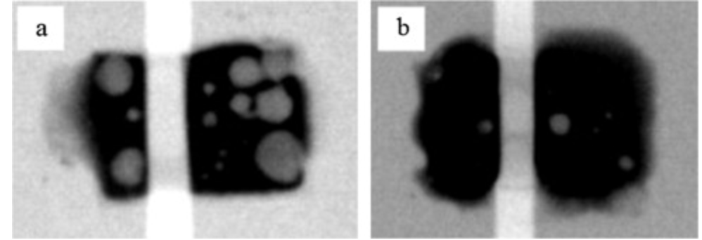
The figure below shows the voiding percentages of LED solder joints corresponding to different thicknesses of solder paste. When the thickness of the solder layer is 20μm and 30μm, the void percentages of the solder joints are 46% and 3%, respectively. Obviously, the volume of solder has a significant influence on the voiding percentage of the solder joint. With an increase in the amount of solder paste, there were no large voids observed in the solder joint, indicating that the solder paste could uniformly contact the chip during the chip placement process.

Figure 2. Void percentage of inverted LED solder joints corresponding to different thicknesses. a: thickness of 20μm, b: thickness of 30μm.
2.3 LED Shear Strength
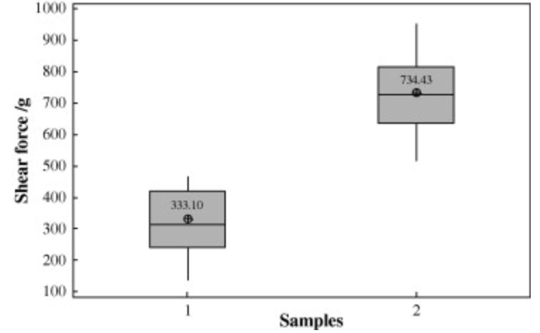
The presence of voids can affect the formation of IMC and reduce the bonding area between the chip and the pad, leading to a weakening of the bond. Therefore, when the void percentage in the solder layer decreases, the shear strength of the LED package increases. In addition, the stress on the solder joint will be concentrated near the voids and gradually lead to cracking.

Figure 3. Shear force of inverted LED solder joints. 1: solder thickness of 20μm, 2: solder thickness of 30μm.
2.4 LED Thermal Performance
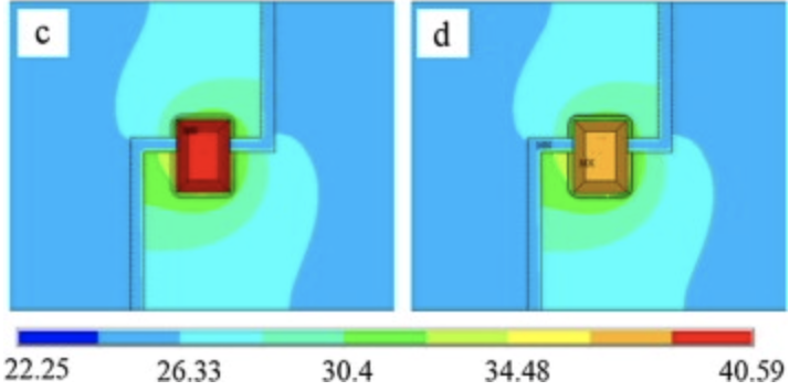
The thermal distribution of the chip under electrical current can be detected by infrared. At 100
Surface temperature of inverted LED

Figure 3. Surface temperature of inverted LED. c: solder thickness 20μm, d: solder thickness 30μm.

